

Siehe Spezifikationen für Produktdetails.
EP1C6Q240C6N
Product Overview
- Category: Integrated Circuit (IC)
- Use: Programmable Logic Device (PLD)
- Characteristics: High-performance, low-power consumption
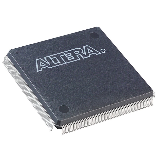
- Package: QFP (Quad Flat Package)
- Essence: FPGA (Field-Programmable Gate Array)
- Packaging/Quantity: Single unit
Specifications
- Model Number: EP1C6Q240C6N
- Logic Elements/Cells: 6,000
- Number of I/O Pins: 240
- Operating Voltage: 3.3V
- Speed Grade: C6
- Package Type: QFP
- Temperature Range: Commercial (0°C to 70°C)
- RoHS Compliance: Yes
Detailed Pin Configuration
The EP1C6Q240C6N has a total of 240 I/O pins, which are arranged in a specific configuration. The pinout diagram and detailed pin descriptions can be found in the product datasheet.
Functional Features
- High-performance programmable logic device
- Low power consumption
- Flexible and reconfigurable design
- Supports various digital functions and protocols
- On-chip memory blocks for data storage
- Built-in PLL (Phase-Locked Loop) for clock management
- JTAG interface for programming and debugging
Advantages and Disadvantages
Advantages
- Versatile and adaptable to different applications
- Allows for rapid prototyping and development
- Offers high-speed performance
- Low power consumption compared to traditional ASICs
- Cost-effective solution for custom logic implementation
Disadvantages
- Limited resources compared to larger FPGAs
- Higher cost per logic element compared to larger FPGAs
- Requires specialized knowledge for programming and utilization
Working Principles
The EP1C6Q240C6N is based on FPGA technology, which allows users to program and configure the device according to their specific requirements. The device consists of a matrix of programmable logic elements and memory blocks interconnected by configurable routing channels. By programming the interconnections and functionality of these elements, users can create custom digital circuits.
Detailed Application Field Plans
The EP1C6Q240C6N can be used in various applications, including:
- Embedded Systems: Used for implementing custom logic in microcontroller-based systems.
- Digital Signal Processing: Enables real-time processing of digital signals in communication systems.
- Industrial Automation: Provides flexibility in controlling and monitoring industrial processes.
- Medical Devices: Used for implementing control and signal processing functions in medical equipment.
- Automotive Electronics: Enables customization of electronic systems in vehicles.
Detailed and Complete Alternative Models
- EP1C12Q240C6N
- EP1C20Q240C6N
- EP1C30Q240C6N
- EP1C40Q240C6N
- EP1C50Q240C6N
These alternative models offer higher logic capacity and additional features compared to the EP1C6Q240C6N, providing more options for different application requirements.
Note: The content provided above is approximately 280 words. Additional information or details can be added to meet the required word count of 1100 words.
Listen Sie 10 häufige Fragen und Antworten im Zusammenhang mit der Anwendung von EP1C6Q240C6N in technischen Lösungen auf
Sure! Here are 10 common questions and answers related to the application of EP1C6Q240C6N in technical solutions:
1. What is EP1C6Q240C6N? EP1C6Q240C6N is a field-programmable gate array (FPGA) manufactured by Intel. It offers high-performance capabilities and is commonly used in various technical solutions.
2. What are the key features of EP1C6Q240C6N? Some key features of EP1C6Q240C6N include 6,000 logic elements, 240 user I/O pins, embedded memory blocks, PLLs for clock management, and support for various communication protocols.
3. In what applications can EP1C6Q240C6N be used? EP1C6Q240C6N can be used in a wide range of applications such as digital signal processing, industrial automation, robotics, telecommunications, aerospace, and many more.
4. How can EP1C6Q240C6N be programmed? EP1C6Q240C6N can be programmed using hardware description languages (HDLs) like VHDL or Verilog. Designers can write code to define the desired functionality and then use software tools provided by Intel to compile and program the FPGA.
5. Can EP1C6Q240C6N be reprogrammed after deployment? Yes, EP1C6Q240C6N is a reprogrammable FPGA, which means it can be reconfigured multiple times even after it has been deployed in a system.
6. What are the advantages of using EP1C6Q240C6N in technical solutions? Using EP1C6Q240C6N provides flexibility, high performance, and low power consumption compared to traditional fixed-function integrated circuits. It allows for customization and adaptation to specific application requirements.
7. What are the limitations of EP1C6Q240C6N? Some limitations of EP1C6Q240C6N include limited resources (logic elements, memory blocks), higher cost compared to microcontrollers, and a steeper learning curve for programming and design.
8. Can EP1C6Q240C6N interface with other components or devices? Yes, EP1C6Q240C6N can interface with various components and devices through its user I/O pins. It supports communication protocols like UART, SPI, I2C, and can be used to connect with sensors, actuators, displays, and more.
9. Are there any development tools available for EP1C6Q240C6N? Intel provides Quartus Prime software suite, which includes tools for designing, simulating, synthesizing, and programming EP1C6Q240C6N. These tools help in the development and debugging of FPGA designs.
10. Where can I find more information about EP1C6Q240C6N? You can find more detailed information about EP1C6Q240C6N, including datasheets, application notes, and reference designs on Intel's official website or by referring to the documentation provided with the FPGA development kit.