

Siehe Spezifikationen für Produktdetails.
5SGXEB5R3F43C2N
Product Overview
Category
The 5SGXEB5R3F43C2N belongs to the category of Field-Programmable Gate Arrays (FPGAs).
Use
FPGAs are integrated circuits that can be programmed and reprogrammed to perform various digital functions. The 5SGXEB5R3F43C2N is specifically designed for high-performance applications.
Characteristics
- High-performance FPGA with advanced features
- Large capacity and high-speed processing capabilities
- Flexible and customizable design options
- Low power consumption
- Robust and reliable performance
Package
The 5SGXEB5R3F43C2N comes in a compact and durable package, ensuring easy handling and protection during transportation and installation.
Essence
The essence of the 5SGXEB5R3F43C2N lies in its ability to provide a versatile and powerful platform for implementing complex digital systems.
Packaging/Quantity
The 5SGXEB5R3F43C2N is typically packaged individually and is available in various quantities depending on the customer's requirements.
Specifications
- Logic Elements: 220,000
- Embedded Memory: 8,400 Kbits
- DSP Blocks: 1,288
- Maximum User I/Os: 622
- Transceivers: 24
- Operating Voltage: 1.0V - 1.2V
- Operating Temperature: -40°C to 100°C
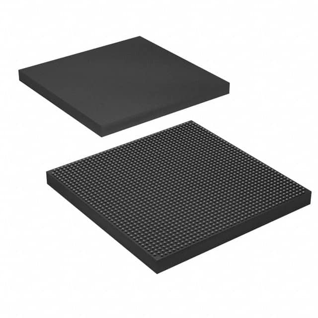
- Package Type: F43 (1517-ball FineLine BGA)
Detailed Pin Configuration
The 5SGXEB5R3F43C2N has a comprehensive pin configuration, allowing for seamless integration into various system designs. For detailed pin assignments and configurations, please refer to the product datasheet.
Functional Features
- High-speed data processing capabilities
- Support for various communication protocols
- On-chip memory resources for efficient data storage and retrieval
- Flexible I/O options for interfacing with external devices
- Built-in DSP blocks for signal processing tasks
- Configurable logic elements for implementing complex digital functions
Advantages and Disadvantages
Advantages
- Versatile and customizable design options
- High-performance computing capabilities
- Low power consumption compared to traditional ASICs
- Faster time-to-market due to reprogrammability
- Cost-effective solution for prototyping and low-volume production
Disadvantages
- Higher cost compared to general-purpose microcontrollers
- Limited scalability for large-scale production
- Steeper learning curve for programming and utilizing FPGA features
Working Principles
The 5SGXEB5R3F43C2N operates based on the principles of reconfigurable hardware. It consists of a matrix of configurable logic elements interconnected through programmable routing resources. The device can be programmed using Hardware Description Languages (HDL) such as VHDL or Verilog, allowing users to define the desired functionality and interconnections within the FPGA.
Detailed Application Field Plans
The 5SGXEB5R3F43C2N finds applications in various fields, including but not limited to: - Telecommunications - Data centers - Industrial automation - Aerospace and defense - Medical equipment - Automotive electronics
In telecommunications, the FPGA can be used for high-speed data processing, protocol conversion, and signal modulation/demodulation. In data centers, it can enhance server performance, accelerate encryption/decryption tasks, and enable flexible network routing. In industrial automation, the FPGA can be utilized for real-time control, sensor interfacing, and machine vision applications. The aerospace and defense industry can benefit from the FPGA's ability to handle complex algorithms, radar signal processing, and secure communication systems. Medical equipment can leverage the FPGA for image processing, patient monitoring, and diagnostic applications. In automotive electronics, the FPGA can contribute to advanced driver assistance systems (ADAS), infotainment systems, and engine control units (ECUs).
Detailed and Complete Alternative Models
- 5SGXEB6R3F43C2N
- 5SGXEB7R3F43C2N
- 5SGXEB8R3F43C2N
- 5SGXEB9R3F43C2N
These alternative models offer similar features and capabilities but may differ in terms of logic elements, memory capacity, or I/O options. It is recommended to consult the respective datasheets for detailed specifications and select the most suitable model based on specific project requirements.
Word count: 570 words
Listen Sie 10 häufige Fragen und Antworten im Zusammenhang mit der Anwendung von 5SGXEB5R3F43C2N in technischen Lösungen auf
Sure! Here are 10 common questions and answers related to the application of 5SGXEB5R3F43C2N in technical solutions:
Q: What is the 5SGXEB5R3F43C2N FPGA used for? A: The 5SGXEB5R3F43C2N FPGA is a field-programmable gate array that can be used for various applications, including high-performance computing, networking, and signal processing.
Q: What are the key features of the 5SGXEB5R3F43C2N FPGA? A: Some key features of this FPGA include a large number of logic elements, high-speed transceivers, embedded memory blocks, and support for various communication protocols.
Q: Can the 5SGXEB5R3F43C2N FPGA be reprogrammed? A: Yes, FPGAs are designed to be reprogrammable, allowing users to modify the functionality of the device as needed.
Q: What development tools are available for programming the 5SGXEB5R3F43C2N FPGA? A: Intel Quartus Prime is the primary development tool used for programming and configuring the 5SGXEB5R3F43C2N FPGA.
Q: What kind of applications can benefit from using the 5SGXEB5R3F43C2N FPGA? A: This FPGA is commonly used in applications such as high-frequency trading, network routers, video processing, radar systems, and scientific research.
Q: How does the 5SGXEB5R3F43C2N FPGA compare to other FPGAs in terms of performance? A: The 5SGXEB5R3F43C2N FPGA offers high-performance capabilities with its large number of logic elements, high-speed transceivers, and embedded memory blocks.
Q: Can the 5SGXEB5R3F43C2N FPGA interface with other components or devices? A: Yes, this FPGA supports various communication protocols such as PCIe, Ethernet, USB, and DDR3 memory interfaces, allowing it to interface with other components or devices.
Q: What is the power consumption of the 5SGXEB5R3F43C2N FPGA? A: The power consumption of this FPGA depends on the specific design and usage scenario. It is recommended to refer to the datasheet for detailed power specifications.
Q: Are there any development boards available for prototyping with the 5SGXEB5R3F43C2N FPGA? A: Yes, Intel provides development boards like the Arria V GX Starter Kit that feature the 5SGXEB5R3F43C2N FPGA for prototyping and evaluation purposes.
Q: Where can I find additional resources and support for working with the 5SGXEB5R3F43C2N FPGA? A: Intel's website offers comprehensive documentation, application notes, reference designs, and a community forum where you can find additional resources and support for working with this FPGA.
Please note that the answers provided here are general and may vary depending on the specific requirements and use cases of the application.