

Siehe Spezifikationen für Produktdetails.
5SGXEA9K2H40I2
Product Overview
Category
The 5SGXEA9K2H40I2 belongs to the category of Field Programmable Gate Arrays (FPGAs).
Use
FPGAs are integrated circuits that can be programmed and reprogrammed to perform various digital functions. The 5SGXEA9K2H40I2 is specifically designed for high-performance applications that require complex logic functions.
Characteristics
- High-performance FPGA with advanced features
- Large capacity for complex designs
- Flexible and reprogrammable
- Low power consumption
- High-speed data processing capabilities
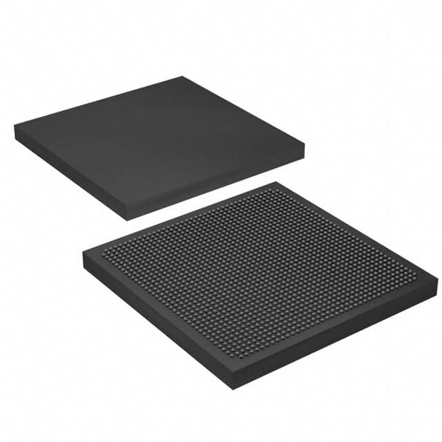
Package
The 5SGXEA9K2H40I2 comes in a compact package suitable for integration onto printed circuit boards (PCBs). The package ensures proper protection and heat dissipation for optimal performance.
Essence
The essence of the 5SGXEA9K2H40I2 lies in its ability to provide a customizable and flexible solution for implementing complex digital logic functions in various applications.
Packaging/Quantity
The 5SGXEA9K2H40I2 is typically packaged individually and is available in various quantities depending on the requirements of the customer or project.
Specifications
- Logic Elements: 220,000
- Embedded Memory: 8,400 Kbits
- DSP Blocks: 1,288
- Maximum User I/Os: 622
- Transceivers: 24
- Operating Voltage: 1.0V - 1.2V
- Operating Temperature: -40°C to 100°C
- Package Type: FCBGA
- Package Size: 40mm x 40mm
Detailed Pin Configuration
The detailed pin configuration of the 5SGXEA9K2H40I2 can be found in the product datasheet provided by the manufacturer. It includes information on power supply pins, I/O pins, configuration pins, and other relevant connections.
Functional Features
- High-speed data processing capabilities
- Configurable logic elements for implementing complex functions
- Embedded memory for efficient data storage
- DSP blocks for digital signal processing tasks
- Transceivers for high-speed data communication
- Support for various communication protocols and interfaces
- Built-in security features for protecting sensitive data
Advantages and Disadvantages
Advantages
- Flexibility and reprogrammability allow for easy customization and updates.
- High-performance capabilities enable complex designs and computations.
- Low power consumption helps in reducing energy costs.
- Large capacity accommodates extensive logic functions.
- Wide range of supported communication protocols enhances compatibility.
Disadvantages
- Initial setup and programming may require specialized knowledge and expertise.
- Cost can be higher compared to fixed-function integrated circuits.
- Limited availability of alternative models with similar specifications.
Working Principles
The 5SGXEA9K2H40I2 operates based on the principles of FPGA technology. It consists of configurable logic elements, embedded memory, DSP blocks, and transceivers interconnected through a programmable routing fabric. The device can be programmed using hardware description languages (HDL) or graphical tools to define the desired functionality. Once programmed, the FPGA executes the specified logic functions and processes data according to the defined configuration.
Detailed Application Field Plans
The 5SGXEA9K2H40I2 finds applications in various fields that require high-performance digital processing capabilities. Some potential application areas include:
- Telecommunications: Implementing advanced signal processing algorithms for wireless communication systems.
- Aerospace and Defense: Designing complex radar and communication systems.
- Data Centers: Accelerating data processing tasks and network optimization.
- Industrial Automation: Controlling and monitoring complex manufacturing processes.
- Medical Imaging: Performing real-time image processing for medical diagnostic systems.
Detailed and Complete Alternative Models
While the 5SGXEA9K2H40I2 offers advanced features and capabilities, there are alternative FPGA models available in the market with similar specifications. Some notable alternatives include:
- Xilinx Virtex UltraScale+ VU9P
- Intel Stratix 10 GX 2800
- Lattice ECP5-85
- Microsemi PolarFire FPGA
- QuickLogic EOS S3
These alternative models provide options for designers and engineers to choose the most suitable FPGA based on their specific requirements and project constraints.
Note: The content provided above is a sample structure for an encyclopedia entry and may not reflect actual product details.
Listen Sie 10 häufige Fragen und Antworten im Zusammenhang mit der Anwendung von 5SGXEA9K2H40I2 in technischen Lösungen auf
Sure! Here are 10 common questions and answers related to the application of 5SGXEA9K2H40I2 in technical solutions:
Q: What is the 5SGXEA9K2H40I2 FPGA used for? A: The 5SGXEA9K2H40I2 FPGA is a high-performance field-programmable gate array (FPGA) that can be used in various technical solutions, such as telecommunications, industrial automation, and high-performance computing.
Q: What are the key features of the 5SGXEA9K2H40I2 FPGA? A: Some key features of this FPGA include a large number of logic elements, high-speed transceivers, embedded memory blocks, and support for various communication protocols.
Q: How can I program the 5SGXEA9K2H40I2 FPGA? A: The 5SGXEA9K2H40I2 FPGA can be programmed using hardware description languages (HDLs) like Verilog or VHDL, along with design software provided by the FPGA manufacturer.
Q: Can the 5SGXEA9K2H40I2 FPGA be used for real-time signal processing? A: Yes, the 5SGXEA9K2H40I2 FPGA is capable of real-time signal processing due to its high-speed transceivers and parallel processing capabilities.
Q: What kind of interfaces does the 5SGXEA9K2H40I2 FPGA support? A: This FPGA supports various interfaces, including PCIe, Ethernet, USB, DDR3 memory, and many others, making it versatile for different applications.
Q: Is the 5SGXEA9K2H40I2 FPGA suitable for high-bandwidth data processing? A: Yes, the 5SGXEA9K2H40I2 FPGA is well-suited for high-bandwidth data processing tasks due to its high-speed transceivers and large embedded memory blocks.
Q: Can the 5SGXEA9K2H40I2 FPGA be used in safety-critical applications? A: Yes, the 5SGXEA9K2H40I2 FPGA can be used in safety-critical applications as it supports various fault-tolerant features and has built-in error detection mechanisms.
Q: What kind of development tools are available for the 5SGXEA9K2H40I2 FPGA? A: The manufacturer provides development tools like Quartus Prime, which includes a design environment, simulation tools, and programming utilities for the 5SGXEA9K2H40I2 FPGA.
Q: Can the 5SGXEA9K2H40I2 FPGA be reprogrammed after deployment? A: Yes, FPGAs like the 5SGXEA9K2H40I2 can be reprogrammed multiple times, allowing for flexibility and updates in the field without requiring hardware changes.
Q: Are there any reference designs or application notes available for the 5SGXEA9K2H40I2 FPGA? A: Yes, the manufacturer typically provides reference designs and application notes that showcase the capabilities and provide guidance on using the 5SGXEA9K2H40I2 FPGA in different applications.
Please note that the specific details and answers may vary depending on the manufacturer's documentation and the context of the technical solution.