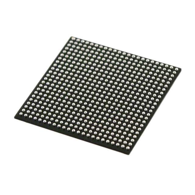
Siehe Spezifikationen für Produktdetails.

5CGXBC4C6U19C7N
Product Overview
Category
The 5CGXBC4C6U19C7N belongs to the category of Field-Programmable Gate Arrays (FPGAs).
Use
This FPGA is designed for various applications that require high-performance and flexible digital logic circuits.
Characteristics
- High-performance: The 5CGXBC4C6U19C7N offers fast processing speeds and low latency, making it suitable for demanding applications.
- Flexibility: Being a field-programmable device, it allows users to configure and reconfigure the logic circuits according to their specific requirements.
- Versatility: The FPGA can be used in a wide range of applications, including telecommunications, automotive, aerospace, and industrial automation.
- Low power consumption: The 5CGXBC4C6U19C7N is designed to minimize power consumption while maintaining high performance.
Package and Quantity
The 5CGXBC4C6U19C7N is available in a compact package, typically measuring 19mm x 19mm. It is supplied in quantities of one unit per package.
Essence
The essence of the 5CGXBC4C6U19C7N lies in its ability to provide a customizable and high-performance digital logic solution for various applications.
Specifications
- Logic Elements: 4,600
- Embedded Memory: 1,638 Kbits
- Maximum User I/Os: 622
- DSP Blocks: 96
- Maximum Operating Frequency: 500 MHz
- Supply Voltage: 1.2V
Detailed Pin Configuration
The 5CGXBC4C6U19C7N has a total of 622 user I/O pins, which are configurable based on the application requirements. These pins are used for input, output, or bidirectional communication with external devices. The pin configuration can be customized using the provided development tools and software.
Functional Features
- High-speed processing: The FPGA offers fast data processing capabilities, making it suitable for real-time applications.
- Reconfigurability: Users can modify the logic circuits within the FPGA to adapt to changing requirements without the need for hardware changes.
- Embedded memory: The 5CGXBC4C6U19C7N includes a significant amount of embedded memory, allowing for efficient data storage and retrieval.
- DSP blocks: The FPGA incorporates dedicated digital signal processing (DSP) blocks, enabling efficient implementation of complex mathematical operations.
Advantages and Disadvantages
Advantages
- Flexibility: The ability to reconfigure the logic circuits provides flexibility in adapting to changing application requirements.
- High performance: The FPGA's fast processing speeds and low latency make it suitable for demanding applications.
- Versatility: The 5CGXBC4C6U19C7N can be used in various industries and applications due to its wide range of features.
Disadvantages
- Complexity: Utilizing FPGAs requires expertise in digital design and programming, which may pose a challenge for beginners.
- Cost: FPGAs tend to be more expensive compared to other integrated circuits due to their programmable nature.
Working Principles
The 5CGXBC4C6U19C7N operates based on the principles of configurable logic. It consists of an array of logic elements that can be interconnected and programmed to perform specific functions. The user configures the FPGA by loading a bitstream, which defines the desired logic circuitry and interconnections. Once programmed, the FPGA executes the configured logic, providing the desired functionality.
Detailed Application Field Plans
The 5CGXBC4C6U19C7N finds applications in various fields, including:
- Telecommunications: The FPGA can be used in network infrastructure equipment, such as routers and switches, to handle high-speed data processing and protocol conversion.
- Automotive: It can be employed in automotive electronics for tasks like advanced driver assistance systems (ADAS), engine control units (ECUs), and infotainment systems.
- Aerospace: FPGAs are utilized in aerospace applications for tasks like radar signal processing, satellite communication, and flight control systems.
- Industrial Automation: The 5CGXBC4C6U19C7N can be integrated into industrial automation systems for tasks like motion control, machine vision, and process monitoring.
Detailed and Complete Alternative Models
- 5CGXFC7D6F31C7N
- 5CGXFC9E6F31C7N
- 5CGXFC5C6F27C7N
- 5CGXFC7C6F27C7N
These alternative models offer similar features and capabilities to the 5CGXBC4C6U19C7N, providing users with
Listen Sie 10 häufige Fragen und Antworten im Zusammenhang mit der Anwendung von 5CGXBC4C6U19C7N in technischen Lösungen auf
Sure! Here are 10 common questions and answers related to the application of 5CGXBC4C6U19C7N in technical solutions:
Q: What is the purpose of the 5CGXBC4C6U19C7N FPGA? A: The 5CGXBC4C6U19C7N is a Field-Programmable Gate Array (FPGA) that can be configured to perform various digital logic functions.
Q: What are some typical applications of the 5CGXBC4C6U19C7N? A: The 5CGXBC4C6U19C7N FPGA is commonly used in telecommunications, industrial automation, automotive, and aerospace industries for tasks like signal processing, data encryption, and control systems.
Q: How does the 5CGXBC4C6U19C7N differ from other FPGAs? A: The 5CGXBC4C6U19C7N belongs to the Intel Cyclone V series and offers a balance between performance, power consumption, and cost-effectiveness.
Q: Can I program the 5CGXBC4C6U19C7N using a high-level programming language? A: Yes, the 5CGXBC4C6U19C7N can be programmed using hardware description languages (HDLs) like VHDL or Verilog, which provide a higher level of abstraction.
Q: What tools do I need to program the 5CGXBC4C6U19C7N? A: You will need a development board, such as the Intel Cyclone V GX Starter Kit, and software tools like Quartus Prime to design, simulate, and program the FPGA.
Q: Can I reprogram the 5CGXBC4C6U19C7N after it has been deployed in a system? A: Yes, FPGAs like the 5CGXBC4C6U19C7N can be reprogrammed multiple times, allowing for flexibility and updates to the system's functionality.
Q: What is the maximum number of logic elements (LEs) in the 5CGXBC4C6U19C7N? A: The 5CGXBC4C6U19C7N contains 41,910 LEs, which are the basic building blocks of the FPGA.
Q: Does the 5CGXBC4C6U19C7N support high-speed serial communication interfaces? A: Yes, the 5CGXBC4C6U19C7N includes transceivers that support protocols like PCIe, Gigabit Ethernet, and USB.
Q: Can the 5CGXBC4C6U19C7N interface with external memory devices? A: Yes, the 5CGXBC4C6U19C7N supports various memory interfaces such as DDR3, DDR2, and QDR II+.
Q: Are there any development resources available for the 5CGXBC4C6U19C7N? A: Yes, Intel provides documentation, reference designs, and online communities where developers can find support and share knowledge about the 5CGXBC4C6U19C7N FPGA.

