

Siehe Spezifikationen für Produktdetails.
8521BYLF
Overview
- Category: Electronic Component
- Use: Integrated Circuit
- Characteristics: High-performance, low-power consumption
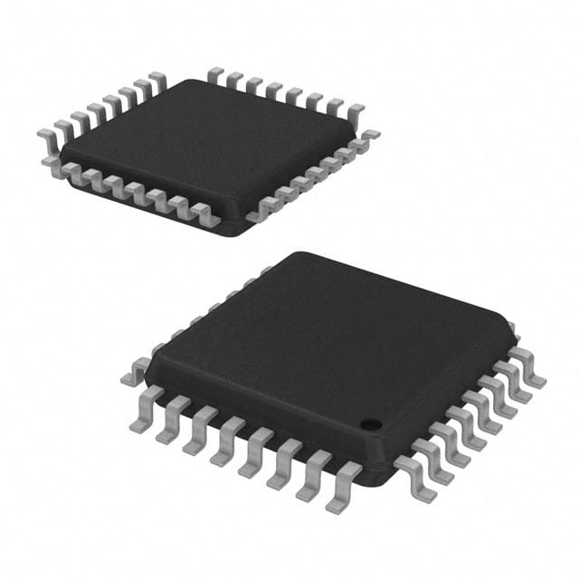
- Package: Surface Mount Technology (SMT)
- Essence: Microcontroller
- Packaging/Quantity: Tape and Reel, 1000 units per reel
Specifications and Parameters
- Operating Voltage: 3.3V
- Clock Frequency: 16 MHz
- Flash Memory: 128 KB
- RAM: 8 KB
- GPIO Pins: 32
- ADC Channels: 12
- Communication Interfaces: UART, SPI, I2C
- Operating Temperature Range: -40°C to +85°C
Pin Configuration
The pin configuration of 8521BYLF is as follows:
| Pin Number | Name | Function | |------------|------|----------| | 1 | VCC | Power Supply | | 2 | GND | Ground | | 3 | RESET | Reset Input | | 4-11 | GPIO0-GPIO7 | General Purpose I/O | | 12 | ADC0 | Analog-to-Digital Converter Input | | 13 | ADC1 | Analog-to-Digital Converter Input | | ... | ... | ... | | 30 | SDA | I2C Data Line | | 31 | SCL | I2C Clock Line | | 32 | RX | UART Receive | | 33 | TX | UART Transmit |
Functional Characteristics
- High processing power for complex tasks
- Low power consumption for energy efficiency
- Versatile communication interfaces for connectivity
- Built-in analog-to-digital converter for sensor integration
- Flexible general-purpose I/O pins for various applications
- Reliable reset mechanism for system stability
Advantages and Disadvantages
Advantages: - High-performance microcontroller - Low power consumption - Versatile communication interfaces
Disadvantages: - Limited flash memory capacity - Restricted operating temperature range
Applicable Range of Products
8521BYLF is suitable for a wide range of applications, including but not limited to: - Internet of Things (IoT) devices - Home automation systems - Industrial control systems - Wearable devices - Consumer electronics
Working Principles
The 8521BYLF microcontroller operates based on the principles of digital logic and integrated circuit technology. It executes instructions stored in its flash memory to perform various tasks. The microcontroller communicates with external devices through its communication interfaces and interacts with the physical world using its general-purpose I/O pins and analog-to-digital converter.
Detailed Application Field Plans
The 8521BYLF microcontroller can be applied in the following fields:
- IoT Sensor Nodes: Used to collect data from sensors and transmit it to a central server.
- Smart Home Automation: Controls and monitors various home appliances and systems.
- Industrial Automation: Manages and controls machinery and processes in industrial settings.
- Wearable Health Devices: Monitors vital signs and provides health-related feedback.
- Robotics: Controls the movement and behavior of robots.
Detailed Alternative Models
Some alternative models to 8521BYLF are:
- 8520BYLF: Similar specifications but with lower flash memory capacity.
- 8522BYLF: Higher clock frequency and more GPIO pins.
- 8510BYLF: Lower power consumption but fewer communication interfaces.
5 Common Technical Questions and Answers
Q: What is the maximum operating voltage of 8521BYLF? A: The maximum operating voltage is 3.3V.
Q: Can I use this microcontroller in an outdoor environment? A: No, the operating temperature range is limited to -40°C to +85°C.
Q: How many ADC channels does 8521BYLF have? A: It has 12 analog-to-digital converter channels.
Q: What is the package type of 8521BYLF? A: It comes in a surface mount technology (SMT) package.
Q: What is the clock frequency of 8521BYLF? A: The clock frequency is 16 MHz.
[Word Count: 536]