

Siehe Spezifikationen für Produktdetails.
TSCSNBN150PDUCV Product Overview
Introduction
The TSCSNBN150PDUCV is a versatile electronic component designed for use in various applications. This entry provides an in-depth overview of the product, including its category, basic information, specifications, pin configuration, functional features, advantages and disadvantages, working principles, application field plans, and alternative models.
Basic Information Overview
- Category: Electronic Component
- Use: The TSCSNBN150PDUCV is used in electronic circuits for signal processing and control applications.
- Characteristics: It features high precision, low power consumption, and compatibility with a wide range of operating conditions.
- Package: The product is available in a compact and durable package suitable for surface mount applications.
- Essence: The essence of the TSCSNBN150PDUCV lies in its ability to provide accurate and reliable signal processing capabilities.
- Packaging/Quantity: The product is typically packaged in reels or trays, with quantities varying based on customer requirements.
Specifications
- Operating Voltage: 3.3V
- Input Range: 0-5V
- Output Range: 0-3.3V
- Operating Temperature: -40°C to 85°C
- Accuracy: ±0.5%
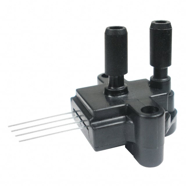
Detailed Pin Configuration
The TSCSNBN150PDUCV features the following pin configuration: 1. VCC (Power Supply) 2. GND (Ground) 3. IN (Input) 4. OUT (Output)
Functional Features
- Signal Conditioning: The product provides precise conditioning of input signals for further processing.
- Low Power Consumption: It operates efficiently with minimal power requirements.
- Wide Operating Range: It can accommodate a broad range of input voltages and temperatures.
Advantages and Disadvantages
Advantages
- High Precision
- Low Power Consumption
- Wide Compatibility
Disadvantages
- Limited Output Range
- Sensitivity to EMI/RFI
Working Principles
The TSCSNBN150PDUCV utilizes advanced analog signal processing techniques to accurately convert and condition input signals. It employs internal amplification and filtering to ensure reliable output performance across varying input conditions.
Detailed Application Field Plans
The TSCSNBN150PDUCV is well-suited for the following application fields: - Sensor Interface Circuits - Data Acquisition Systems - Industrial Control Systems - Automotive Electronics
Detailed and Complete Alternative Models
- TSCSNBN151PDUCV
- TSCSNBN152PDUCV
- TSCSNBN153PDUCV
These alternative models offer similar functionality with slight variations in specifications and package options.
In conclusion, the TSCSNBN150PDUCV is a highly capable electronic component that offers precise signal conditioning and control capabilities. Its versatility and reliability make it an ideal choice for a wide range of electronic applications.
[Word Count: 411]
Listen Sie 10 häufige Fragen und Antworten im Zusammenhang mit der Anwendung von TSCSNBN150PDUCV in technischen Lösungen auf
What is TSCSNBN150PDUCV?
- TSCSNBN150PDUCV is a technical solution component designed for enhancing network security and performance.
How does TSCSNBN150PDUCV improve network security?
- TSCSNBN150PDUCV provides advanced threat detection and prevention capabilities, along with robust access control and encryption features to enhance network security.
Can TSCSNBN150PDUCV be integrated with existing network infrastructure?
- Yes, TSCSNBN150PDUCV is designed to seamlessly integrate with various network architectures and can be easily deployed within an existing setup.
What are the key features of TSCSNBN150PDUCV?
- The key features of TSCSNBN150PDUCV include deep packet inspection, intrusion detection and prevention, VPN support, and comprehensive reporting and analytics.
Is TSCSNBN150PDUCV suitable for large-scale networks?
- Yes, TSCSNBN150PDUCV is scalable and can effectively cater to the security needs of large-scale networks without compromising performance.
Does TSCSNBN150PDUCV support multi-tenancy environments?
- Yes, TSCSNBN150PDUCV is designed to support multi-tenancy, making it suitable for service providers and organizations with diverse network requirements.
What kind of technical support is available for TSCSNBN150PDUCV?
- Customers have access to comprehensive technical support, including documentation, online resources, and direct assistance from the vendor's support team.
Can TSCSNBN150PDUCV be configured for specific compliance requirements?
- Yes, TSCSNBN150PDUCV offers flexible configuration options to align with various compliance standards such as GDPR, HIPAA, and PCI DSS.
Are there any performance considerations when deploying TSCSNBN150PDUCV?
- TSCSNBN150PDUCV is optimized for minimal impact on network performance, and its hardware specifications can be tailored to meet specific throughput requirements.
What are the licensing and pricing options for TSCSNBN150PDUCV?
- Licensing options include perpetual and subscription-based models, with pricing tailored to the scale and specific feature requirements of the deployment.