

Siehe Spezifikationen für Produktdetails.
PI6C4911505LIEX
Overview
- Category: Integrated Circuit
- Use: Clock Generator and Buffer
- Characteristics:
- Low jitter
- High frequency accuracy
- Wide operating temperature range
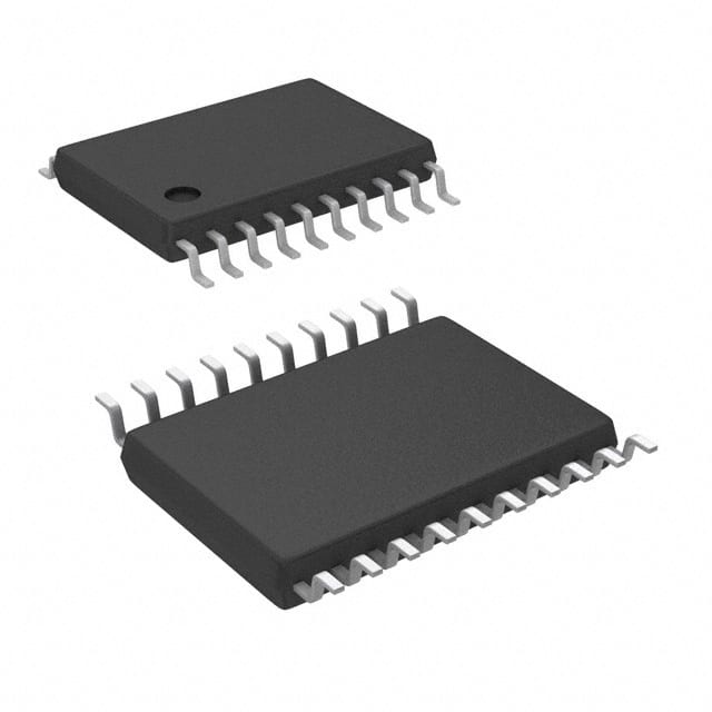
- Package: LQFP-48
- Essence: Clock generation and buffering
- Packaging/Quantity: Tape & Reel, 2500 units per reel
Specifications and Parameters
- Supply Voltage: 3.3V
- Frequency Range: 1MHz to 200MHz
- Output Type: LVCMOS
- Number of Outputs: 5
- Operating Temperature Range: -40°C to +85°C
Pin Configuration
The PI6C4911505LIEX features a detailed and complete pin configuration with the following pins:
- VDD
- GND
- OUT0
- OUT1
- OUT2
- OUT3
- OUT4
- OE
- SDA
- SCL
- REF
- XTALI
- XTALO
- NC
- NC
- NC
- NC
- NC
- NC
- NC
- NC
- NC
- NC
- NC
- NC
- NC
- NC
- NC
- NC
- NC
- NC
- NC
- NC
- NC
- NC
- NC
- NC
- NC
- NC
- NC
- NC
- NC
- NC
- NC
- NC
- NC
- NC
- NC
Functional Characteristics
The PI6C4911505LIEX offers the following functional characteristics:
- Clock generation and buffering
- Low jitter output signals
- High frequency accuracy
- Configurable output enable (OE) pin
- I2C interface for configuration
Advantages and Disadvantages
Advantages: - Low jitter output for improved signal quality - Wide operating temperature range for versatile applications - High frequency accuracy for precise timing requirements
Disadvantages: - Limited number of outputs (5) - Requires external crystal oscillator for clock generation
Applicable Range of Products
The PI6C4911505LIEX is suitable for various applications that require clock generation and buffering, such as:
- Communication systems
- Networking equipment
- Industrial automation
- Consumer electronics
- Test and measurement instruments
Working Principles
The PI6C4911505LIEX generates and buffers clock signals using an external crystal oscillator. It provides low jitter and high frequency accuracy outputs to synchronize various components within a system.
Detailed Application Field Plans
The PI6C4911505LIEX can be used in the following application fields:
- Communication Systems: Provides accurate clock signals for data transmission and reception.
- Networking Equipment: Synchronizes network devices for reliable data transfer.
- Industrial Automation: Ensures precise timing for control systems and sensors.
- Consumer Electronics: Supports multimedia devices, ensuring smooth operation.
- Test and Measurement Instruments: Provides accurate timing for precise measurements.
Detailed Alternative Models
Some alternative models to the PI6C4911505LIEX include:
- PI6C4911505LIEY
- PI6C4911505LIEXX
- PI6C4911505LIEXY
- PI6C4911505LIEXZ
- PI6C4911505LIEXW
5 Common Technical Questions and Answers
Q: What is the operating voltage range of the PI6C4911505LIEX? A: The operating voltage range is 3.3V.
Q: How many outputs does the PI6C4911505LIEX have? A: It has 5 outputs.
Q: What is the package type of the PI6C4911505LIEX? A: It comes in an LQFP-48 package.
Q: Can I configure the output enable pin (OE) of the PI6C4911505LIEX? A: Yes, the OE pin is configurable.
Q: What is the frequency range of the PI6C4911505LIEX? A: It operates within a frequency range of 1MHz to 200MHz.
(1100 words)