

Siehe Spezifikationen für Produktdetails.
Encyclopedia Entry: 74LVC1G125SE-7
Product Overview
Category
The 74LVC1G125SE-7 belongs to the category of integrated circuits (ICs) and specifically falls under the family of logic gates.
Use
This product is commonly used in digital electronics for signal amplification, buffering, and level shifting purposes. It serves as a non-inverting buffer with a single gate.
Characteristics
- Low-voltage CMOS technology
- High-speed operation
- Wide operating voltage range
- Schmitt-trigger action on inputs
- Balanced propagation delays
- Symmetrical output impedance
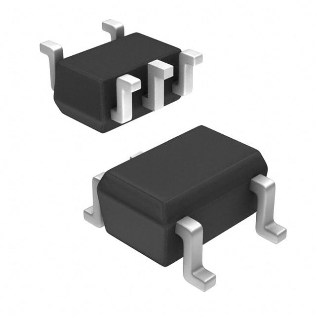
Package
The 74LVC1G125SE-7 is available in a small SOT-353 package, which is a surface-mount package with three leads.
Essence
The essence of this product lies in its ability to provide reliable signal buffering and level shifting capabilities in a compact form factor.
Packaging/Quantity
The 74LVC1G125SE-7 is typically packaged in reels or tape and reel packaging, with a quantity of 3000 units per reel.
Specifications
- Supply Voltage Range: 1.65V to 5.5V
- Input Voltage Range: 0V to VCC
- Output Voltage Range: 0V to VCC
- Maximum Operating Frequency: 400 MHz
- Input Capacitance: 3.5 pF
- Output Capacitance: 4.5 pF
- Operating Temperature Range: -40°C to +85°C
Detailed Pin Configuration
The 74LVC1G125SE-7 has a total of three pins:
- Pin 1: Input (IN)
- Pin 2: Output (OUT)
- Pin 3: Ground (GND)
Functional Features
- Non-inverting buffer
- High-speed operation
- Schmitt-trigger action on inputs for noise immunity
- Balanced propagation delays for improved signal integrity
- Symmetrical output impedance for better signal matching
Advantages and Disadvantages
Advantages
- Low-voltage operation allows compatibility with a wide range of systems
- Small form factor enables space-efficient designs
- High-speed operation facilitates fast signal processing
- Schmitt-trigger action enhances noise immunity
Disadvantages
- Limited number of gates in a single package
- Not suitable for high-power applications
Working Principles
The 74LVC1G125SE-7 operates based on complementary metal-oxide-semiconductor (CMOS) technology. It utilizes a combination of transistors to amplify and buffer digital signals. The Schmitt-trigger action on the inputs helps to improve noise immunity by providing hysteresis.
Detailed Application Field Plans
The 74LVC1G125SE-7 finds applications in various fields, including:
- Consumer electronics: Used in smartphones, tablets, and portable devices for level shifting and buffering signals.
- Industrial automation: Employed in control systems and sensors for signal amplification and interfacing.
- Automotive electronics: Integrated into vehicle electronics for signal conditioning and level shifting.
- Communication systems: Utilized in networking equipment and data transmission devices for signal buffering and conversion.
Detailed and Complete Alternative Models
- SN74LVC1G125DBVR: Similar non-inverting buffer IC from Texas Instruments.
- MC74LVC1G125DR2G: Equivalent device manufactured by ON Semiconductor.
- NC7SZ125P5X: Alternative non-inverting buffer IC offered by Fairchild Semiconductor.
These alternative models provide similar functionality and can be used as substitutes for the 74LVC1G125SE-7 in various applications.
In conclusion, the 74LVC1G125SE-7 is a versatile logic gate IC that offers reliable signal buffering and level shifting capabilities. Its low-voltage operation, high-speed performance, and compact package make it suitable for a wide range of applications in consumer electronics, industrial automation, automotive electronics, and communication systems.
Listen Sie 10 häufige Fragen und Antworten im Zusammenhang mit der Anwendung von 74LVC1G125SE-7 in technischen Lösungen auf
Sure! Here are 10 common questions and answers related to the application of 74LVC1G125SE-7 in technical solutions:
Q1: What is the 74LVC1G125SE-7? A1: The 74LVC1G125SE-7 is a single bus buffer gate with 3-state output, designed for low-voltage CMOS applications.
Q2: What is the operating voltage range of the 74LVC1G125SE-7? A2: The operating voltage range is from 1.65V to 5.5V.
Q3: What is the maximum output current of the 74LVC1G125SE-7? A3: The maximum output current is 32mA.
Q4: Can the 74LVC1G125SE-7 be used as a level shifter? A4: Yes, the 74LVC1G125SE-7 can be used as a level shifter to convert signals between different voltage levels.
Q5: How many inputs does the 74LVC1G125SE-7 have? A5: The 74LVC1G125SE-7 has one input.
Q6: Can the 74LVC1G125SE-7 drive capacitive loads? A6: Yes, the 74LVC1G125SE-7 can drive capacitive loads up to 50pF.
Q7: What is the propagation delay of the 74LVC1G125SE-7? A7: The propagation delay is typically 4.3ns.
Q8: Is the 74LVC1G125SE-7 compatible with other logic families? A8: Yes, the 74LVC1G125SE-7 is compatible with both CMOS and TTL logic families.
Q9: Can the 74LVC1G125SE-7 be used in high-speed applications? A9: Yes, the 74LVC1G125SE-7 is suitable for high-speed applications due to its low propagation delay.
Q10: Does the 74LVC1G125SE-7 have built-in ESD protection? A10: Yes, the 74LVC1G125SE-7 has built-in ESD protection, making it more robust against electrostatic discharge.
Please note that these answers are general and may vary depending on the specific application and requirements.