

Siehe Spezifikationen für Produktdetails.
Encyclopedia Entry: 74AHC1G125SE-7
Product Overview
Category
The 74AHC1G125SE-7 belongs to the category of integrated circuits (ICs).
Use
This IC is commonly used for signal buffering and level shifting in various electronic devices and systems.
Characteristics
- Low power consumption
- High-speed operation
- Wide operating voltage range
- Schmitt-trigger input for noise immunity
- Compatible with both CMOS and TTL logic levels
Package
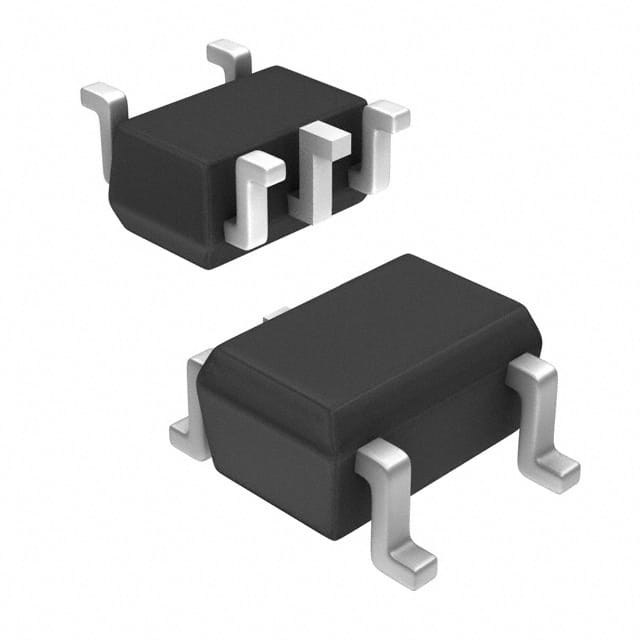
The 74AHC1G125SE-7 is available in a small SOT-23 package, which is suitable for space-constrained applications.
Essence
The essence of this product lies in its ability to provide reliable signal buffering and level shifting capabilities in a compact form factor.
Packaging/Quantity
The 74AHC1G125SE-7 is typically packaged in reels or tubes, containing a quantity of 3000 units per reel/tube.
Specifications
- Supply Voltage Range: 2.0V to 5.5V
- Input Voltage Range: -0.5V to VCC + 0.5V
- Output Voltage Range: GND to VCC
- Operating Temperature Range: -40°C to +125°C
- Output Drive Capability: ±8mA at VCC = 3.0V
Detailed Pin Configuration
The 74AHC1G125SE-7 has a total of 5 pins: 1. Pin 1: Input (I) 2. Pin 2: Output (O) 3. Pin 3: Ground (GND) 4. Pin 4: Power Supply (VCC) 5. Pin 5: Enable (E)
Functional Features
- Single gate buffer with tri-state output
- Non-inverting buffer
- High-speed operation for efficient signal transmission
- Schmitt-trigger input for improved noise immunity
- Output can be disabled using the enable pin (E)
Advantages and Disadvantages
Advantages
- Low power consumption makes it suitable for battery-powered devices
- Wide operating voltage range allows compatibility with various systems
- Small package size enables use in space-constrained applications
- Schmitt-trigger input enhances noise immunity
Disadvantages
- Limited output drive capability may not be suitable for high-current applications
- Single gate configuration may restrict certain complex circuit designs
Working Principles
The 74AHC1G125SE-7 operates by receiving an input signal at the input pin (I), which is then buffered and level-shifted to the output pin (O). The output can be enabled or disabled using the enable pin (E). The IC utilizes CMOS technology to achieve low power consumption and high-speed operation.
Detailed Application Field Plans
The 74AHC1G125SE-7 finds applications in various electronic systems, including but not limited to: - Mobile devices - Consumer electronics - Industrial automation - Automotive electronics - Communication systems
Detailed and Complete Alternative Models
Some alternative models that offer similar functionality to the 74AHC1G125SE-7 include: - SN74LVC1G125DBVR - MC74VHC1GT125DF2G - TC7SZ125FU
These alternatives can be considered based on specific requirements and availability.
In conclusion, the 74AHC1G125SE-7 is a versatile integrated circuit that provides signal buffering and level shifting capabilities. Its low power consumption, high-speed operation, and compact package make it suitable for a wide range of applications in various industries.
Listen Sie 10 häufige Fragen und Antworten im Zusammenhang mit der Anwendung von 74AHC1G125SE-7 in technischen Lösungen auf
Sure! Here are 10 common questions and answers related to the application of 74AHC1G125SE-7 in technical solutions:
Q1: What is the function of the 74AHC1G125SE-7? A1: The 74AHC1G125SE-7 is a single bus buffer gate with 3-state output. It is used to control the flow of data between different parts of a circuit.
Q2: What is the voltage supply range for the 74AHC1G125SE-7? A2: The voltage supply range for the 74AHC1G125SE-7 is typically between 2V and 5.5V.
Q3: How many inputs does the 74AHC1G125SE-7 have? A3: The 74AHC1G125SE-7 has one input.
Q4: How many outputs does the 74AHC1G125SE-7 have? A4: The 74AHC1G125SE-7 has one output.
Q5: What is the maximum output current of the 74AHC1G125SE-7? A5: The maximum output current of the 74AHC1G125SE-7 is typically 8mA.
Q6: Can the 74AHC1G125SE-7 be used in high-speed applications? A6: Yes, the 74AHC1G125SE-7 is designed for high-speed applications and has a typical propagation delay of 4.5ns.
Q7: Is the 74AHC1G125SE-7 compatible with other logic families? A7: Yes, the 74AHC1G125SE-7 is compatible with both CMOS and TTL logic families.
Q8: Can the 74AHC1G125SE-7 be used in both input and output applications? A8: Yes, the 74AHC1G125SE-7 can be used as both an input buffer and an output driver.
Q9: What is the operating temperature range for the 74AHC1G125SE-7? A9: The operating temperature range for the 74AHC1G125SE-7 is typically between -40°C and 125°C.
Q10: Is the 74AHC1G125SE-7 available in different package options? A10: Yes, the 74AHC1G125SE-7 is available in various package options, such as SOT23 and SC-70.
Please note that the answers provided here are general and may vary depending on the specific datasheet and manufacturer's specifications.