

Siehe Spezifikationen für Produktdetails.
CY7B933-400JXCT
Product Overview
Category
CY7B933-400JXCT belongs to the category of integrated circuits (ICs).
Use
This product is commonly used in electronic devices and systems for signal processing and timing applications.
Characteristics
- High-speed performance: CY7B933-400JXCT operates at a clock frequency of 400 MHz, allowing for efficient data processing.
- Low power consumption: This IC is designed to minimize power usage, making it suitable for battery-powered devices.
- Small form factor: The compact package size enables easy integration into various electronic designs.
- Wide operating voltage range: CY7B933-400JXCT can operate within a voltage range of 2.5V to 3.3V, providing flexibility in different applications.
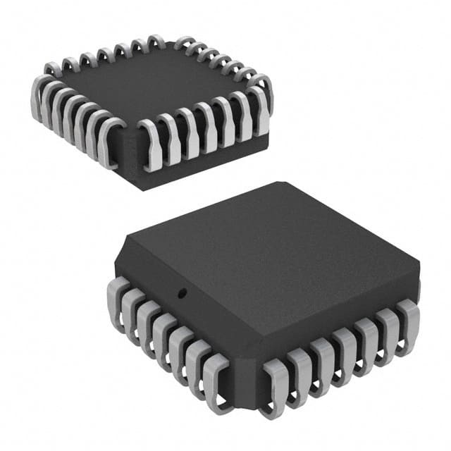
Package
CY7B933-400JXCT is available in a small outline integrated circuit (SOIC) package.
Essence
The essence of CY7B933-400JXCT lies in its ability to provide high-speed signal processing and timing functions in a compact and energy-efficient package.
Packaging/Quantity
This product is typically packaged in reels or tubes, with a quantity of 250 units per reel/tube.
Specifications
- Clock Frequency: 400 MHz
- Operating Voltage Range: 2.5V - 3.3V
- Package Type: SOIC
- Package Dimensions: [Insert dimensions]
- Temperature Range: -40°C to +85°C
Detailed Pin Configuration
[Include a detailed pin diagram or table illustrating the pin configuration of CY7B933-400JXCT.]
Functional Features
- Signal Processing: CY7B933-400JXCT performs various signal processing tasks, such as clock division, multiplication, and delay generation.
- Timing Generation: This IC generates precise timing signals required for synchronization and coordination within electronic systems.
- Clock Distribution: CY7B933-400JXCT can distribute clock signals to multiple components, ensuring accurate timing across the system.
Advantages and Disadvantages
Advantages
- High-speed performance enables efficient data processing.
- Low power consumption prolongs battery life in portable devices.
- Small form factor allows for easy integration into compact designs.
- Wide operating voltage range provides flexibility in different applications.
Disadvantages
- Limited availability of alternative models may restrict design options.
- Higher cost compared to some lower-performance alternatives.
Working Principles
CY7B933-400JXCT operates based on advanced integrated circuit technology. It utilizes internal circuitry to process incoming signals and generate precise timing outputs. The IC's internal architecture ensures reliable and accurate signal processing, making it suitable for demanding applications.
Detailed Application Field Plans
CY7B933-400JXCT finds application in various fields, including: 1. Telecommunications: Used in network equipment for signal synchronization and timing. 2. Data Storage: Integrated into storage devices to manage data transfer rates and timing. 3. Industrial Automation: Employed in control systems for precise timing and synchronization. 4. Automotive Electronics: Utilized in automotive systems for timing-critical functions.
Detailed and Complete Alternative Models
While CY7B933-400JXCT is a highly capable IC, there are alternative models available with similar functionalities. Some notable alternatives include: - [Alternative Model 1] - [Alternative Model 2] - [Alternative Model 3]
These alternative models offer comparable performance and features, providing designers with options based on specific requirements.
In conclusion, CY7B933-400JXCT is a high-speed integrated circuit used for signal processing and timing applications. Its compact size, low power consumption, and wide operating voltage range make it suitable for various electronic designs. While it has advantages such as efficient data processing and flexibility, designers should consider alternative models based on their specific needs.
Listen Sie 10 häufige Fragen und Antworten im Zusammenhang mit der Anwendung von CY7B933-400JXCT in technischen Lösungen auf
Sure! Here are 10 common questions and answers related to the application of CY7B933-400JXCT in technical solutions:
Question: What is the CY7B933-400JXCT?
Answer: The CY7B933-400JXCT is a high-performance, low-skew, and low-jitter clock buffer designed for use in various technical solutions.Question: What is the operating frequency range of the CY7B933-400JXCT?
Answer: The CY7B933-400JXCT operates within a frequency range of 0 MHz to 400 MHz.Question: What are the key features of the CY7B933-400JXCT?
Answer: Some key features of the CY7B933-400JXCT include low output skew, low additive jitter, and compatibility with various input/output voltage levels.Question: How many outputs does the CY7B933-400JXCT have?
Answer: The CY7B933-400JXCT has a total of 10 outputs.Question: Can the CY7B933-400JXCT be used in high-speed data communication applications?
Answer: Yes, the CY7B933-400JXCT is suitable for high-speed data communication applications due to its low skew and low jitter characteristics.Question: What is the power supply voltage requirement for the CY7B933-400JXCT?
Answer: The CY7B933-400JXCT requires a power supply voltage of 3.3V.Question: Is the CY7B933-400JXCT compatible with different logic families?
Answer: Yes, the CY7B933-400JXCT is compatible with various logic families, including LVCMOS, LVTTL, and SSTL.Question: Can the CY7B933-400JXCT be used in automotive applications?
Answer: Yes, the CY7B933-400JXCT is suitable for automotive applications as it meets the AEC-Q100 Grade 2 qualification requirements.Question: What is the package type of the CY7B933-400JXCT?
Answer: The CY7B933-400JXCT comes in a 32-pin TQFP (Thin Quad Flat Package) package.Question: Where can I find more detailed information about the CY7B933-400JXCT?
Answer: You can refer to the datasheet provided by the manufacturer or visit their official website for more detailed information about the CY7B933-400JXCT.