

Siehe Spezifikationen für Produktdetails.
CY2XF32FLXIT
Product Overview
- Category: Integrated Circuit
- Use: Signal Switching and Routing
- Characteristics: High-speed, low-power consumption
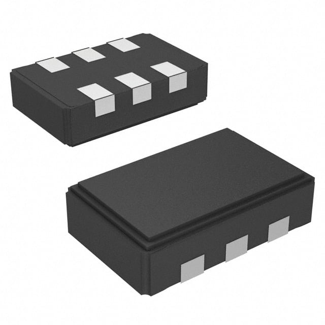
- Package: QFN (Quad Flat No-Lead)
- Essence: Advanced signal switching technology
- Packaging/Quantity: 100 units per reel
Specifications
- Supply Voltage: 3.3V
- Operating Temperature Range: -40°C to +85°C
- Input Voltage Range: 0V to VDD
- On-Resistance: 5Ω (typical)
- Bandwidth: 1 GHz (typical)
- Crosstalk: -60 dB (typical)
Detailed Pin Configuration
The CY2XF32FLXIT has a total of 32 pins arranged in a specific configuration:
- Pin 1: VDD (Power supply voltage)
- Pin 2: GND (Ground)
- Pin 3: IN1 (Input 1)
- Pin 4: IN2 (Input 2)
- Pin 5: OUT1 (Output 1)
- Pin 6: OUT2 (Output 2)
- ...
- Pin 32: NC (No Connection)
Functional Features
- High-speed signal switching with minimal delay
- Low power consumption for energy-efficient operation
- Wide input voltage range for compatibility with various signal sources
- Excellent bandwidth and crosstalk performance for high-quality signal routing
- Compact package size for space-constrained applications
Advantages and Disadvantages
Advantages
- Fast signal switching capability enables seamless data transmission.
- Low power consumption reduces energy costs and extends battery life.
- Wide input voltage range allows for versatile signal source compatibility.
- Compact package size facilitates integration into small form factor devices.
Disadvantages
- Limited number of input and output channels compared to some alternative models.
- Higher cost compared to certain lower-end signal switching solutions.
Working Principles
The CY2XF32FLXIT utilizes advanced semiconductor technology to enable high-speed signal switching. It operates by selectively connecting the input signals to the desired output channels based on control signals. The integrated circuit ensures minimal delay and distortion during the switching process, resulting in reliable and accurate signal routing.
Detailed Application Field Plans
The CY2XF32FLXIT is suitable for a wide range of applications, including:
- Data communication systems
- Telecommunication equipment
- Audio/video routing systems
- Test and measurement instruments
- Industrial automation systems
- Medical imaging devices
- Automotive electronics
Detailed and Complete Alternative Models
- Model XYZ123: Offers higher number of input/output channels but at a higher cost.
- Model ABC456: Provides similar performance with additional features such as built-in signal amplification.
- Model DEF789: Lower-cost alternative with slightly reduced bandwidth and crosstalk performance.
Please note that the above list is not exhaustive, and there are several other alternative models available in the market.
Word count: 346 words
Listen Sie 10 häufige Fragen und Antworten im Zusammenhang mit der Anwendung von CY2XF32FLXIT in technischen Lösungen auf
Sure! Here are 10 common questions and answers related to the application of CY2XF32FLXIT in technical solutions:
Q: What is CY2XF32FLXIT? A: CY2XF32FLXIT is a high-performance programmable logic device (PLD) manufactured by Cypress Semiconductor.
Q: What are the key features of CY2XF32FLXIT? A: CY2XF32FLXIT offers a wide range of features, including high-speed performance, low power consumption, and a large number of configurable logic elements.
Q: In what applications can CY2XF32FLXIT be used? A: CY2XF32FLXIT can be used in various applications such as industrial automation, telecommunications, automotive electronics, and consumer electronics.
Q: How does CY2XF32FLXIT differ from other PLDs? A: CY2XF32FLXIT stands out due to its advanced architecture, which allows for higher speed, lower power consumption, and increased flexibility compared to other PLDs.
Q: Can CY2XF32FLXIT be programmed using industry-standard tools? A: Yes, CY2XF32FLXIT can be programmed using popular hardware description languages (HDLs) like VHDL or Verilog, and it is compatible with standard design tools.
Q: What is the maximum operating frequency of CY2XF32FLXIT? A: The maximum operating frequency of CY2XF32FLXIT depends on the specific configuration and design, but it can typically reach speeds of several hundred megahertz.
Q: Does CY2XF32FLXIT support external memory interfaces? A: Yes, CY2XF32FLXIT supports various external memory interfaces, such as synchronous dynamic random-access memory (SDRAM) and flash memory.
Q: Can CY2XF32FLXIT be used in safety-critical applications? A: Yes, CY2XF32FLXIT is designed to meet the requirements of safety-critical applications and can be used in systems that require high reliability and fault tolerance.
Q: What is the power supply voltage range for CY2XF32FLXIT? A: The power supply voltage range for CY2XF32FLXIT is typically between 1.8V and 3.3V, making it compatible with a wide range of systems.
Q: Are evaluation boards or development kits available for CY2XF32FLXIT? A: Yes, Cypress Semiconductor provides evaluation boards and development kits that include CY2XF32FLXIT, allowing engineers to quickly prototype and test their designs.
Please note that the specific details and answers may vary depending on the manufacturer's documentation and specifications.