

Siehe Spezifikationen für Produktdetails.
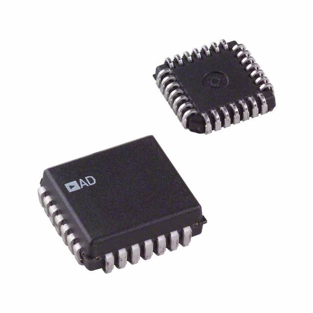
AD7569JP
Product Overview
- Category: Analog-to-Digital Converter (ADC)
- Use: Converts analog signals into digital data
- Characteristics: High resolution, low power consumption
- Package: DIP (Dual In-line Package)
- Essence: Precise conversion of analog signals to digital format
- Packaging/Quantity: Individually packaged, quantity per package varies
Specifications
- Resolution: 16 bits
- Input Voltage Range: ±10V
- Sampling Rate: 100 kSPS (Samples per Second)
- Power Supply: +5V
- Operating Temperature Range: -40°C to +85°C
Detailed Pin Configuration
The AD7569JP has a total of 28 pins. The pin configuration is as follows:
- VREF-
- VREF+
- AGND
- DGND
- VIN-
- VIN+
- VDD
- VSS
- D0
- D1
- D2
- D3
- D4
- D5
- D6
- D7
- D8
- D9
- D10
- D11
- D12
- D13
- D14
- D15
- CS
- RD
- WR
- A0
Functional Features
- High-resolution conversion with 16-bit accuracy
- Low power consumption for energy-efficient operation
- Wide input voltage range allows for versatile signal conversion
- Fast sampling rate ensures real-time data acquisition
- Easy integration with microcontrollers and other digital systems
Advantages and Disadvantages
Advantages: - High resolution provides accurate digital representation of analog signals - Low power consumption reduces energy usage and heat generation - Versatile input voltage range allows for compatibility with various signal sources - Fast sampling rate enables real-time data acquisition
Disadvantages: - Limited number of input channels - Requires external voltage reference for precise conversion
Working Principles
The AD7569JP utilizes a successive approximation register (SAR) architecture to convert analog signals into digital data. The input voltage is compared to a reference voltage, and the converter determines the digital representation based on the comparison results. The conversion process is controlled by the internal circuitry, which ensures accurate and reliable conversion.
Detailed Application Field Plans
The AD7569JP is commonly used in applications that require high-resolution analog-to-digital conversion. Some potential application fields include:
- Industrial Automation: Precise measurement and control systems
- Medical Equipment: Data acquisition from sensors and transducers
- Test and Measurement: Accurate data capture for analysis and evaluation
- Audio Processing: Conversion of analog audio signals into digital format
- Instrumentation: Signal processing and analysis in scientific instruments
Detailed and Complete Alternative Models
- AD7689JP: 18-bit resolution ADC with similar features
- AD7791JP: Low-power, 24-bit resolution ADC for precision applications
- AD7476JP: 12-bit resolution ADC with integrated multiplexer
- AD7091RJP: 12-bit resolution ADC with built-in temperature sensor
- AD7606JP: 16-channel, simultaneous sampling ADC for multi-channel applications
(Note: This list is not exhaustive and there may be other alternative models available.)
Word count: 335 words
Listen Sie 10 häufige Fragen und Antworten im Zusammenhang mit der Anwendung von AD7569JP in technischen Lösungen auf
Sure! Here are 10 common questions and answers related to the application of AD7569JP in technical solutions:
Q: What is AD7569JP? A: AD7569JP is a specific model of analog-to-digital converter (ADC) manufactured by Analog Devices.
Q: What is the purpose of an ADC? A: An ADC converts analog signals into digital data, allowing for processing and analysis in digital systems.
Q: What are the key features of AD7569JP? A: AD7569JP offers 12-bit resolution, simultaneous sampling on all channels, low power consumption, and a wide input voltage range.
Q: What applications can AD7569JP be used for? A: AD7569JP is commonly used in industrial automation, data acquisition systems, medical equipment, and instrumentation.
Q: How many channels does AD7569JP support? A: AD7569JP has 8 differential input channels, which can be configured as single-ended inputs if needed.
Q: What is the maximum sampling rate of AD7569JP? A: AD7569JP supports a maximum sampling rate of 200 kilosamples per second (ksps).
Q: What is the supply voltage range for AD7569JP? A: AD7569JP operates with a supply voltage range of 2.7V to 5.25V.
Q: Does AD7569JP have built-in reference voltage options? A: Yes, AD7569JP provides both internal and external reference voltage options for flexibility in different applications.
Q: Can AD7569JP operate in harsh environments? A: Yes, AD7569JP is designed to operate in extended temperature ranges and is suitable for use in harsh industrial environments.
Q: What interface does AD7569JP use for communication? A: AD7569JP utilizes a serial peripheral interface (SPI) for communication with microcontrollers or other digital devices.
Please note that these answers are general and may vary depending on the specific requirements and configurations of your technical solution.