

Siehe Spezifikationen für Produktdetails.
AS7C256A-20TIN
Product Overview
Category
AS7C256A-20TIN belongs to the category of semiconductor memory devices.
Use
This product is primarily used for data storage in various electronic devices such as computers, smartphones, and embedded systems.
Characteristics
- High-speed operation: AS7C256A-20TIN offers fast access times, allowing for efficient data retrieval.
- Large storage capacity: With a capacity of 256 kilobits (32 kilobytes), this memory device can store a significant amount of data.
- Low power consumption: The AS7C256A-20TIN is designed to consume minimal power, making it suitable for battery-powered devices.
- Reliable performance: This product ensures reliable data storage and retrieval, minimizing the risk of data loss or corruption.
Package
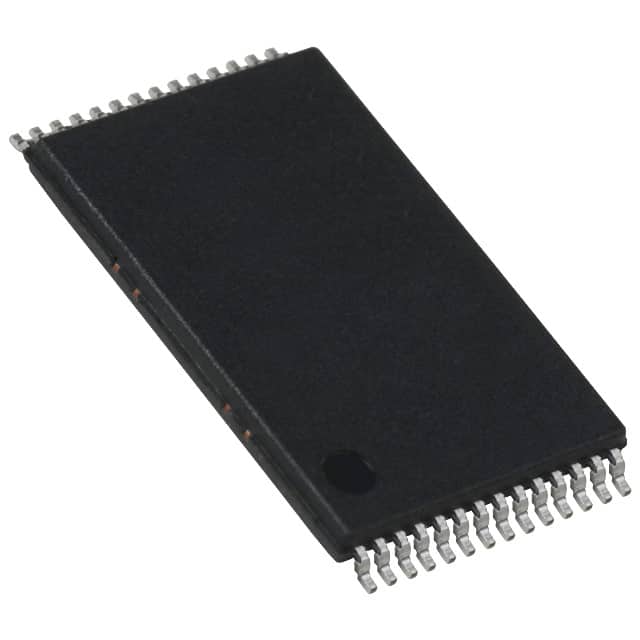
AS7C256A-20TIN is available in a Thin Small Outline Package (TSOP), which provides a compact and space-saving form factor.
Essence
The essence of AS7C256A-20TIN lies in its ability to provide high-speed and reliable data storage in electronic devices.
Packaging/Quantity
This product is typically packaged in reels, with each reel containing a specific quantity of AS7C256A-20TIN units. The exact quantity may vary depending on the manufacturer's specifications.
Specifications
- Operating Voltage: 3.0V - 3.6V
- Access Time: 20 nanoseconds
- Organization: 32K x 8 bits
- Standby Current: 10 microamps (typical)
- Operating Temperature Range: -40°C to +85°C
Detailed Pin Configuration
The AS7C256A-20TIN has a total of 28 pins, each serving a specific function. Here is a detailed pin configuration:
- A0 - Address Input
- A1 - Address Input
- A2 - Address Input
- A3 - Address Input
- A4 - Address Input
- A5 - Address Input
- A6 - Address Input
- A7 - Address Input
- CE - Chip Enable Input
- OE - Output Enable Input
- WE - Write Enable Input
- I/O0 - Data Input/Output
- I/O1 - Data Input/Output
- I/O2 - Data Input/Output
- I/O3 - Data Input/Output
- Vcc - Power Supply
- GND - Ground
- I/O4 - Data Input/Output
- I/O5 - Data Input/Output
- I/O6 - Data Input/Output
- I/O7 - Data Input/Output
- NC - No Connection
- NC - No Connection
- NC - No Connection
- NC - No Connection
- NC - No Connection
- NC - No Connection
- NC - No Connection
Functional Features
- Random Access: AS7C256A-20TIN allows for random access to any memory location, enabling efficient data retrieval.
- Low Power Consumption: This product is designed to minimize power consumption during both active and standby modes, prolonging battery life in portable devices.
- High Reliability: AS7C256A-20TIN ensures reliable data storage and retrieval, reducing the risk of data corruption or loss.
- Compatibility: This memory device is compatible with various microcontrollers and processors, making it versatile for different applications.
Advantages and Disadvantages
Advantages
- Fast access times enable quick data retrieval.
- Large storage capacity accommodates a significant amount of data.
- Low power consumption prolongs battery life in portable devices.
- Reliable performance ensures data integrity.
Disadvantages
- Limited storage capacity compared to higher-capacity memory devices.
- Higher cost per kilobit compared to larger memory chips.
Working Principles
AS7C256A-20TIN operates based on the principles of semiconductor memory technology. It utilizes a combination of electronic circuits and storage cells to store and retrieve digital data. The memory cells within the device are organized into an array, with each cell capable of storing one bit of information. The address inputs control the selection of specific memory locations, while the control inputs (CE, OE, WE) manage the read and write operations.
Detailed Application Field Plans
AS7C256A-20TIN finds applications in various fields, including:
- Computers: Used as cache memory or for storing system firmware.
- Smartphones and Tablets: Provides additional storage for apps, media files, and user data.
- Embedded Systems: Utilized for program storage in microcontrollers and other embedded devices.
- Automotive Electronics: Used for data storage in infotainment systems, navigation units,
Listen Sie 10 häufige Fragen und Antworten im Zusammenhang mit der Anwendung von AS7C256A-20TIN in technischen Lösungen auf
Sure! Here are 10 common questions and answers related to the application of AS7C256A-20TIN in technical solutions:
Question: What is AS7C256A-20TIN?
- Answer: AS7C256A-20TIN is a specific model of SRAM (Static Random Access Memory) chip with a capacity of 256 kilobits.Question: What is the operating voltage range for AS7C256A-20TIN?
- Answer: The operating voltage range for AS7C256A-20TIN is typically between 4.5V and 5.5V.Question: What is the maximum clock frequency supported by AS7C256A-20TIN?
- Answer: AS7C256A-20TIN can support a maximum clock frequency of 20 MHz.Question: Can AS7C256A-20TIN be used in battery-powered devices?
- Answer: Yes, AS7C256A-20TIN can be used in battery-powered devices as it operates within a typical voltage range suitable for such applications.Question: What is the access time of AS7C256A-20TIN?
- Answer: The access time of AS7C256A-20TIN is typically 20 ns.Question: Is AS7C256A-20TIN compatible with both commercial and industrial temperature ranges?
- Answer: Yes, AS7C256A-20TIN is designed to operate within both commercial (0°C to 70°C) and industrial (-40°C to 85°C) temperature ranges.Question: Can AS7C256A-20TIN be used in high-reliability applications?
- Answer: Yes, AS7C256A-20TIN is suitable for high-reliability applications as it has a high endurance and can withstand harsh operating conditions.Question: What is the package type of AS7C256A-20TIN?
- Answer: AS7C256A-20TIN comes in a 28-pin Thin Small Outline Package (TSOP).Question: Can AS7C256A-20TIN be used in automotive electronics?
- Answer: Yes, AS7C256A-20TIN is designed to meet the requirements of automotive electronics and can be used in such applications.Question: Is AS7C256A-20TIN pin-compatible with other SRAM chips?
- Answer: AS7C256A-20TIN follows industry-standard pinout configurations and is generally pin-compatible with other SRAM chips of similar capacity and package type.
Please note that the answers provided here are general and may vary depending on specific datasheet specifications and application requirements.