

Siehe Spezifikationen für Produktdetails.
AT25DF021A-MHN-T
Product Overview
- Category: Flash Memory
- Use: Data storage and retrieval in electronic devices
- Characteristics: Non-volatile, high-density, low-power consumption
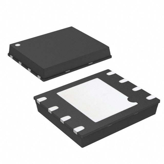
- Package: 8-pin SOIC (Small Outline Integrated Circuit)
- Essence: Serial Flash Memory
- Packaging/Quantity: Tape and Reel, 2500 units per reel
Specifications
- Memory Size: 2 Megabits (256 Kilobytes)
- Interface: Serial Peripheral Interface (SPI)
- Operating Voltage: 2.7V to 3.6V
- Operating Temperature Range: -40°C to +85°C
- Write Endurance: 100,000 cycles
- Data Retention: 20 years
- Page Size: 256 bytes
- Sector Size: 4 kilobytes
- Erase Time: 35 milliseconds (typical)
Pin Configuration
The AT25DF021A-MHN-T has the following pin configuration:
- Chip Select (/CS)
- Serial Clock (SCK)
- Serial Data Input (SI)
- Serial Data Output (SO)
- Write Protect (/WP)
- Hold (/HOLD)
- VCC (Power Supply)
- Ground (GND)
Functional Features
- High-speed data transfer with SPI interface
- Sector erase and page program operations
- Software and hardware write protection options
- Deep power-down mode for ultra-low power consumption
- Continuous read mode for efficient data retrieval
Advantages and Disadvantages
Advantages: - Compact package size for space-constrained applications - Low power consumption extends battery life - High-density memory allows for ample data storage - Fast data transfer speeds improve system performance
Disadvantages: - Limited write endurance compared to other memory technologies - Relatively small page and sector sizes may require additional management in certain applications
Working Principles
The AT25DF021A-MHN-T is based on the Serial Peripheral Interface (SPI) protocol. It utilizes a non-volatile memory technology that retains data even when power is disconnected. The SPI interface enables high-speed communication between the memory and the host device, allowing for efficient data storage and retrieval.
Detailed Application Field Plans
The AT25DF021A-MHN-T is commonly used in various electronic devices, including but not limited to:
- Consumer Electronics: Smartphones, tablets, digital cameras
- Automotive Systems: Infotainment systems, instrument clusters
- Industrial Equipment: Measurement devices, control systems
- Medical Devices: Patient monitoring systems, diagnostic equipment
- Internet of Things (IoT): Connected devices, sensors
Detailed and Complete Alternative Models
- AT25DF041A-MHN-T: 4 Megabit (512 Kilobytes) capacity
- AT25DF081A-MHN-T: 8 Megabit (1 Megabyte) capacity
- AT25DF161A-MHN-T: 16 Megabit (2 Megabytes) capacity
- AT25DF321A-MHN-T: 32 Megabit (4 Megabytes) capacity
- AT25DF641A-MHN-T: 64 Megabit (8 Megabytes) capacity
These alternative models offer increased memory capacities while maintaining similar characteristics and functionality.
Word count: 410 words
Listen Sie 10 häufige Fragen und Antworten im Zusammenhang mit der Anwendung von AT25DF021A-MHN-T in technischen Lösungen auf
Sure! Here are 10 common questions and answers related to the application of AT25DF021A-MHN-T in technical solutions:
Q: What is the AT25DF021A-MHN-T? A: The AT25DF021A-MHN-T is a serial flash memory chip manufactured by Adesto Technologies. It has a capacity of 2 megabits (256 kilobytes) and operates on a Serial Peripheral Interface (SPI).
Q: What are some typical applications for the AT25DF021A-MHN-T? A: This flash memory chip is commonly used in various embedded systems, IoT devices, consumer electronics, automotive applications, and industrial control systems.
Q: What voltage does the AT25DF021A-MHN-T operate at? A: The AT25DF021A-MHN-T operates at a voltage range of 2.7V to 3.6V.
Q: What is the maximum data transfer rate supported by this flash memory chip? A: The AT25DF021A-MHN-T supports a maximum data transfer rate of up to 85 MHz.
Q: Does the AT25DF021A-MHN-T support both read and write operations? A: Yes, it supports both read and write operations, allowing you to store and retrieve data from the flash memory.
Q: Can I erase specific sectors of the AT25DF021A-MHN-T? A: Yes, the AT25DF021A-MHN-T supports sector erase operations, which allow you to erase specific sectors of the flash memory.
Q: Is the AT25DF021A-MHN-T resistant to data loss during power outages? A: Yes, it features a built-in power-loss protection mechanism that ensures data integrity during power interruptions.
Q: What is the typical endurance of the AT25DF021A-MHN-T? A: The AT25DF021A-MHN-T has a typical endurance of 100,000 write cycles per sector.
Q: Can I operate the AT25DF021A-MHN-T in a wide temperature range? A: Yes, this flash memory chip is designed to operate reliably in a wide temperature range, typically from -40°C to +85°C.
Q: Does the AT25DF021A-MHN-T support software and hardware protection features? A: Yes, it offers both software and hardware protection mechanisms, such as write protection and block locking, to prevent unauthorized access or modification of data.
Please note that these answers are based on general information about the AT25DF021A-MHN-T and may vary depending on specific implementation details and requirements.